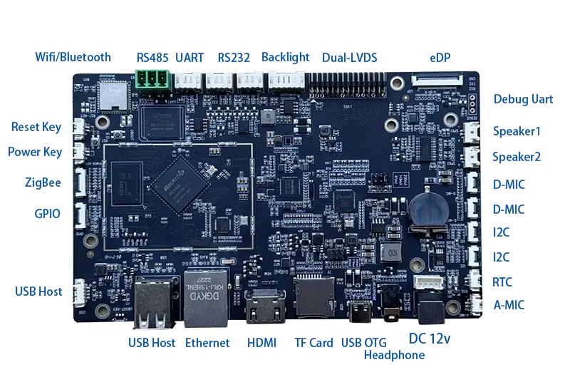
In embedded hardware design, single-board computers (SBCs) are typically rectangular. This shape simplifies manufacturing, EMC layout, and enclosure design. However, in real-world product development, constraints imposed by industrial housing and interface layout may force engineers to break the rule—and embrace irregular-shaped PCBs.
In this post, I’ll share our recent experience designing a custom Android/Linux SBC that couldn’t be a rectangle. This journey highlights how structure, space, and interfaces come together to reshape the board—literally.
🧩 1. Project Background
Our client required:
- A smart embedded device installed inside a non-standard plastic housing.
- Interfaces like display, buttons, camera, speaker, mic, USB, serial, and Ethernet exposed in different directions.
- Extremely limited internal space—no room for a standard rectangular PCB.
The challenge: fragmented space and tight interface orientation constraints meant a typical SBC layout simply wouldn't fit.
🛠️ 2. Design Considerations
After evaluating various options, we settled on these core principles:
- Interface-first layout: Interface positions defined the layout priorities.
- Core concentration: SoC, PMIC, and memory were clustered for better thermal and shielding design.
- No sub-boards: To reduce cost and improve reliability, all interfaces were on a single PCB.
- Shape follows housing: The final board was “T-shaped,” matching the inner contour of the housing.
📐 3. PCB Layout & Design Tricks
To make it work, we used several advanced techniques:
- Isolated power zones for each functional module
- EMC precautions around extended ports, including extra ground shielding and TVS protection
- Irregular PCB edge matching with enclosure mold tolerances
- Mechanical-electrical co-design using SolidWorks + Altium for alignment
Signal integrity was ensured via differential routing, solid ground planes, and copper fill optimization.
🧪 4. Assembly & Prototype Validation
We created a 3D-printed housing + PCB mockup for the first test fit—this helped us avoid costly mold changes. After full assembly, all interfaces aligned perfectly, and no mechanical stress was observed.
The prototype passed thermal, EMI, and reliability tests including extended burn-in and field simulation.
🧾 5. Conclusion
While irregular-shaped PCBs increase design complexity, they offer practical benefits in space-constrained, interface-heavy products:
- Meet industrial design needs
- Enable higher integration in tight spaces
- Avoid reliability issues from multiple sub-boards
In the future, non-rectangular SBCs may become more common as embedded devices shrink and diversify. Engineers must balance structure, thermals, signal layout, and manufacturability to achieve robust designs.
💬 Working on a custom SBC? Want to avoid the same headaches we went through?
Check out our full suite of embedded solutions:

