In an FPGA (Field-Programmable Gate Array), Configurable Logic Blocks (CLBs) are the fundamental building blocks that implement digital logic functions. Their interconnection determines the FPGA's functionality. Here’s how CLBs are connected to realize any desired functionality:
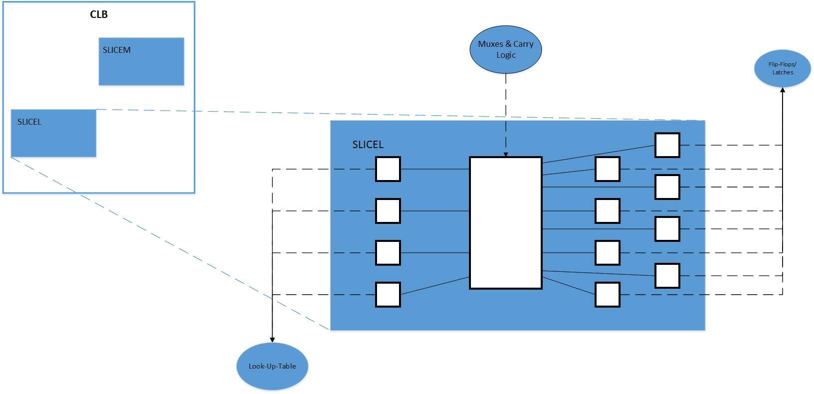
1. CLB Structure (Basic Components)
A typical CLB consists of:
Look-Up Tables (LUTs):
- Store truth tables for combinational logic (e.g., AND, OR, XOR).
- A 6-input LUT can implement any 6-input Boolean function.
Flip-Flops (FFs):
Store state for sequential logic (e.g., registers, counters).
Multiplexers (MUXes):
Route signals within the CLB.
Carry Logic:
Optimizes arithmetic operations (e.g., adders, counters).
2. How CLBs Are Connected
FPGAs use a programmable interconnect network to link CLBs and other resources (I/O blocks, DSPs, etc.). The process involves:
A. Intra-CLB Connections
LUTs ↔ Flip-Flops:
Combinational outputs from LUTs can be registered by FFs for synchronous logic.
Carry Chain Routing:
Dedicated paths between CLBs for fast arithmetic operations.
B. Inter-CLB Connections
Switch Matrices:
Programmable switches connect CLB outputs to horizontal/vertical routing channels.
Routing Channels:
Wires of varying lengths (local, intermediate, global) for signal propagation.
Clock Networks:
Low-skew global routes for clock signals.
C. Hierarchical Routing
- Local Routing: Within a single CLB (e.g., LUT → FF).
- Neighbor Routing: Between adjacent CLBs (short wires).
- Global Routing: Across the FPGA (longer wires for high-fanout signals).
3. Example: Implementing a 4-Bit Adder
Step 1: Logic Mapping
Each full adder (1-bit) is mapped to a CLB:
- LUT computes SUM = A ⊕ B ⊕ Cin.
- Another LUT computes Cout = (A ∧ B) ∨ (Cin ∧ (A ⊕ B)).
Step 2: CLB Interconnection
Carry chains link CLBs to propagate Cout to the next adder.
Step 3: Routing
- Inputs (A, B, Cin) routed via switch matrices.
- Outputs (SUM, Cout) sent to other CLBs or I/O pins.
4. Tools Involved
Synthesis: Converts HDL (VHDL/Verilog) to LUT/FF-level netlists.
Place & Route (P&R):
- Placement: Assigns logic to specific CLBs.
- Routing: Configures switches to connect CLBs.
Bitstream Generation: Creates a configuration file for the FPGA.
5. Key Concepts
Flexibility: Any function can be implemented by programming LUTs and interconnects.
Trade-offs:
- More logic = More CLBs used → Higher latency/power.
- Long routes = Signal delay → Timing constraints matter.
Modern Enhancements:
Heterogeneous blocks (DSPs, BRAMs) for optimized performance.
Visualization
CLB1 (LUT+FF) → Switch Matrix → Routing Channel → CLB2 (LUT+FF)
                   ↑
               Global Clock
Conclusion
FPGAs achieve functionality by:
- Breaking logic into LUTs/FFs within CLBs.
- Using programmable interconnects to route signals between CLBs.
- Optimizing placement/routing to meet timing/power goals.